520.492 Mixed-Signal VLSI Systems
Title of your project
Your Names
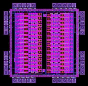
This should be a screendump
of the layout of your chip (top view).
Objectives
A short description of what your chip tries to do, and what approach you followed. Keep it to the point.
Specifications
A quantitative description of what your chip is designed to do. Include a block diagram of your chip that is sufficiently descriptive of the operation. Insert graphics to do so. A Cadence screendump may work; however it must be more than a collection of boxes and wires.
Include a table with the pin diagram of the chip, and explain briefly the function, e.g.: Vbiasn is the nMOS bias voltage for the source followers.
|
1 |
Vbiasn |
40 |
|
|
2 |
Vbiasp |
39 |
|
|
3 |
|
38 |
|
|
4 |
|
37 |
|
|
5 |
|
36 |
|
|
6 |
|
35 |
|
|
7 |
|
34 |
|
|
8 |
|
33 |
|
|
9 |
|
32 |
|
|
10 |
|
31 |
|
|
11 |
|
30 |
|
|
12 |
|
29 |
|
|
13 |
|
28 |
|
|
14 |
|
27 |
|
|
15 |
|
26 |
|
|
16 |
|
25 |
|
|
17 |
|
24 |
|
|
18 |
|
23 |
|
|
19 |
|
22 |
|
|
20 |
|
21 |
|
Circuits
Describe the operation of your chip by showing and explaining key circuit diagrams. The description should be self-contained, but refer to the literature for standard and well-known circuits [1] rather than replicating them here.
Results
Document some of the (simulation) results you got.
References
[1] Any reference worth pointing to.
[2] Another one.