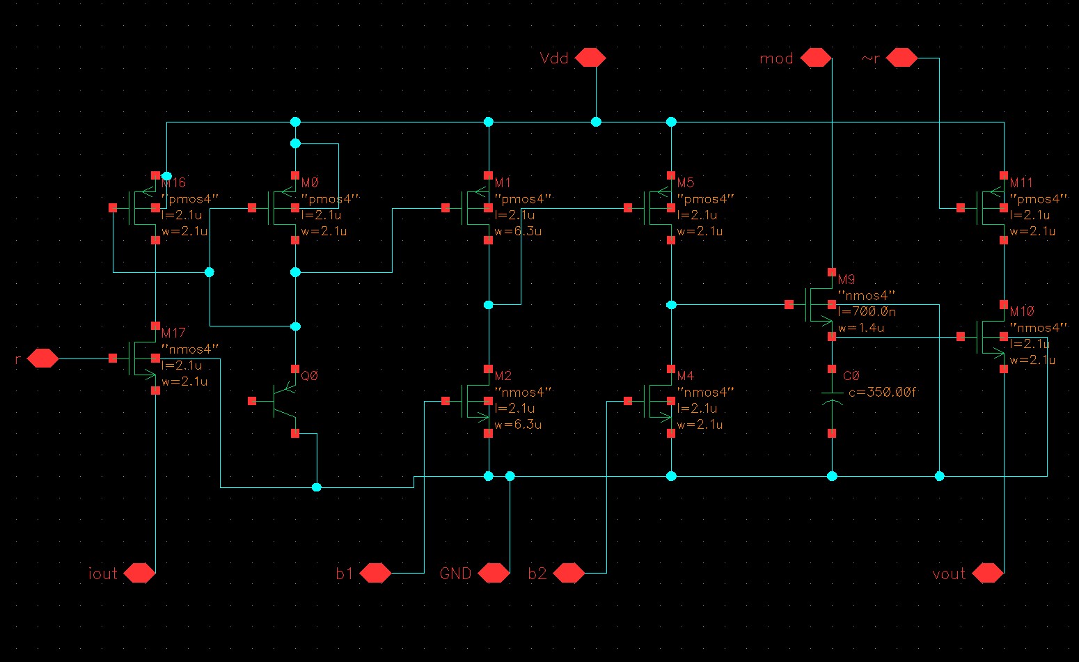
Figure 2.1.1 The schematic for a pixel. Note PNP transistor has floating input, as this is the photosensitive region.
The inputs are;
r, row select
~r, row not select
b1, the bias voltage for the first inverting amplifier
b2, the bias voltage for the second inverting amplifier
mod, the modulation signal
The outputs are;
Iout, the copy of the phototransistor current
Vout, the sampled modulation signal voltage