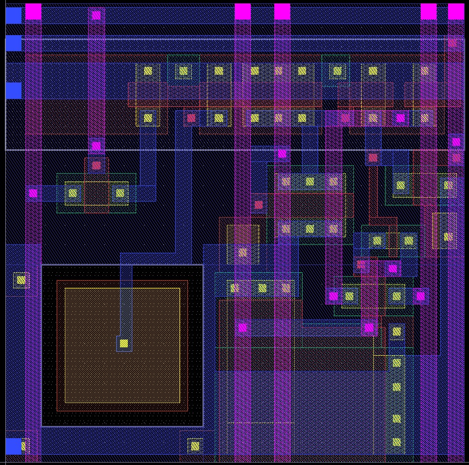
Figure 2.1.2 The layout for a pixel. Note PNP at lower left and S/H capacitor at lower right.
The horizontal metal 1 lines are (from top to bottom);
r, row select
~r, row not select
Vdd
GND
The Vertical metal 2 lines are (from left to right);
Iout, the copy of the phototransistor current
mod, the modulation signal
b1, the bias voltage for the first inverting amplifier
Vout, the sampled modulation signal voltage
b2, the bias voltage for the second inverting amplifier