Figure 2.3.1 The layout for an output buffer cell.
The pass gate is on the left. The horizontal wires are, from top to
bottom, Vdd, Output Voltage buffer Bias Voltage 1,
Output Voltage buffer Bias Voltage 2, GND, Vout, Iout
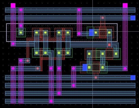
Figure 2.3.1 The layout for an output buffer cell. The pass gate is on the left. The horizontal wires are, from top to bottom, Vdd, Output Voltage buffer Bias Voltage 1, Output Voltage buffer Bias Voltage 2, GND, Vout, Iout