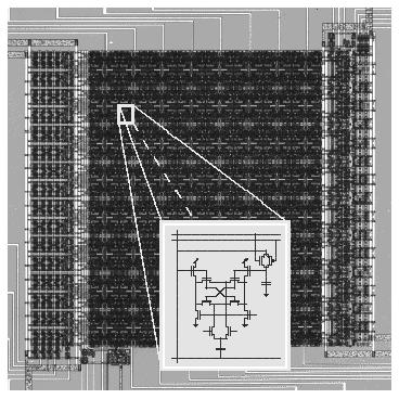
Figure 1: \ Parallel VLSI implementation of an analog vector quantizer. The chip operates directly on analog vectorial data, and produces a digital output code in a single clock cycle.
In Proc. 9th
Annual IEEE International ASIC Conference, Rochester NY, Sept. 1996, pp
273-278 (invited paper).
Copyright, IEEE, 1996.
Gert Cauwenberghs
Electrical and Computer Engineering
Johns Hopkins University, Baltimore, MD 21218
E-mail: gert@bach.ece.jhu.edu
Abstract-- Adaptation and learning are key elements in biological and artificial neural systems for computational tasks of perception, classification, association, and control. They also provide an effective means to compensate for imprecisions in highly efficient analog VLSI implementations of parallel application-specific processors, which offer real-time operation and low power dissipation. The effectiveness of embedded learning and adaptive functions in analog VLSI relies on careful design of the implemented adaptive algorithms, and on adequate means for local and long-term analog memory storage of the adapted parameter coefficients. We address issues of technology, algorithms, and architecture in analog VLSI adaptation and learning, and illustrate those with examples of prototyped ASIC processors.
The field of ``neuromorphic engineering" [1] has been introduced by Carver Mead as an interdisciplinary approach to the design of biologically inspired neural information processing systems, whereby models of perception and information processing in biological systems are mapped onto analog VLSI systems that not only emulate their functions but also resemble their structure. The analog VLSI implementation medium uses MOS transistors operating in the subthreshold region for a high dynamic range of currents and high energetic efficiency [2], and uses parallel distributed architectures for low-power, real-time and robust operation [3].
Mechanisms of adaptation and learning are crucial to the design of neuromorphic VLSI systems, which not only need to emulate functions of plasticity found in biological neural systems, but also need to provide a means to compensate for analog imperfections in the physical implementation and fluctuations in the environment in which they operate. Examples of early implementations of analog VLSI neural systems with integrated adaptation and learning functions can be found in [4].
The analog VLSI neuromorphic computational paradigm extends to the design of efficient parallel ASIC processors implementing a more general class of signal and information processing functions, including focal-plane active pixel imagers, acoustic processors, pattern classifiers, and coders/decoders. The paradigm applies wherever low-power dissipation and real-time operation are important design criteria, and can be simply summarized as follows:
Figure 1: \
Parallel VLSI implementation of an analog vector quantizer. The chip operates
directly on analog vectorial data, and produces a digital output code in a
single clock cycle.
An example illustrating the analog parallel computing paradigm is illustrated
in Figure 1 [5]. The vector quantizer (VQ) performs all
computations in parallel in a single clock cycle, using global summing of
charges in the distance computation and global communication of the winning
voltage level in the winner-take-all selection. The inset of
Figure 1 shows an instance of the circuit cell implementing the VQ
distance computations. The cell measures 78 ![]() m by 60
m by 60 ![]() m in 2
m in 2 ![]() m
CMOS, and dissipates less than 10 pJ energy per cycle.
m
CMOS, and dissipates less than 10 pJ energy per cycle.
Owing to their distributed parallel architecture, systems under the analog computing paradigm are robust to noise and random errors in the environment in which they operate. Additionally, robustness to temporal variability of the environment can be achieved through on-line adaptation of the system parameters. Furthermore, analog imprecisions in the physical implementation of the computational functions (such as those caused by transistor mismatches and device nonlinearities) can be compensated through adaptation of the system parameters as well, provided the number of parameters constitute sufficient degrees of freedom to do so. This is the case for connectionist neural network structures, where every synapse constitutes a free parameter.
The general framework for adaptation and learning is depicted in
Figure 2. An adaptive element adjusts the parameters ![]() (vector
(vector ![]() ) of the system (such as an ASIC processor embedded in its
operational environment) to minimize an error index
) of the system (such as an ASIC processor embedded in its
operational environment) to minimize an error index ![]() that
quantifies a measure of performance (or lack thereof):
that
quantifies a measure of performance (or lack thereof):
![]()
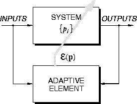
Figure 2: \
Adaptation and learning in a computational system (ASIC processor embedded in
application environment) by adjusting the analog system parameters ![]() to
optimize the performance index
to
optimize the performance index ![]() .
.
Learning can be broadly defined as a higher form of adaptation whereby past
experience is used effectively in readjusting the response of the system to
previously unseen, although similar, input stimuli. The distinct objective in
learning is to generalize beyond the specifics of the presented input
samples, and minimize the expected value of ![]() from the
underlying statistics of the training samples:
from the
underlying statistics of the training samples:
![]()
Based on the nature and availability of a training feedback signal in the
formulation of ![]() , learning algorithms for artificial neural
networks fall under three broad categories: unsupervised [6],
supervised [7] and reward/punishment
(reinforcement) [8]. For example, supervised learning assumes that
a ``teacher" is continuously available to produce target values
, learning algorithms for artificial neural
networks fall under three broad categories: unsupervised [6],
supervised [7] and reward/punishment
(reinforcement) [8]. For example, supervised learning assumes that
a ``teacher" is continuously available to produce target values
![]() for the outputs
for the outputs ![]() , whereby the (instantaneous)
error index is quantified as the distance between actual and target outputs
, whereby the (instantaneous)
error index is quantified as the distance between actual and target outputs
using a distance metric with norm ![]() .
.
On-chip learning in analog VLSI has proven to be a challenging task for several reasons. First, learning algorithms that are efficiently implemented on general-purpose digital computers do not necessarily map efficiently onto analog VLSI hardware. Second, even if the learning algorithm supports a parallel and scalable architecture suitable for analog VLSI implementation, inaccuracies in the implementation of the adaptive functions themselves may significantly affect the performance of the trained system. Finally, practical use necessitates an effective means to retain the parameter values after adaptation, in the form of local analog memory storage. These challenges are addressed in the following sections.
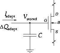
Figure 3: \
Adaptation and memory in analog VLSI: storage node with MOS charge buffer and
adaptive element. Volatile storage due to ohmic contact with the adaptive
element requires dynamic refresh to retain the stored value. Non-volatile
storage avoids ohmic contact by capacitive coupling with the adaptive element.
Adaptation and learning in analog VLSI are inherently coupled with mechanisms of analog storage. In VLSI, analog parameters are conveniently stored as charge or voltage on a capacitor, connecting to the insulating gate of an MOS transistor which serves as a buffer between storage of the parameter and the function it performs. A capacitive memory is generically depicted in Figure 3. An adaptive element updates the stored parameter in the form of discrete charge increments
where ![]() .
.
On itself, a floating gate capacitor is a perfect memory. Non-volatile adaptive elements interface with the floating gate capacitor by capacitive coupling across an insulating oxide. The charge remains, except during adaptation (4), when charge transport through the oxide is activated by tunneling and hot electron injection [9] or UV-excited conduction [10],[11]. In contrast, the parameter value drifts spontaneously due to leakage when the capacitor is in volatile contact with the adaptive element, such as through drain or source terminals of MOS transistors. The short-term nature of volatile storage requires a dynamic refresh mechanism to achieve long-term memory stability [12], [13]. However, autonomous dynamic refresh can be effectively implemented using the same local VLSI hardware resources already provided to implement the adaptive functions (4), demonstrated below.
Gradient descent is a commonly used iterative optimization technique that
minimizes the error index ![]() by incremental updates in the parameter vector
by incremental updates in the parameter vector
![]() :
:
Application of the chain rule for differentation to calculate the gradient
of (3) in feedforward networks yields the popular ``backpropagation"
algorithm [7]. Stated more generally, for supervised as well
as unsupervised learning, the update increment of a given weight parameter
connecting two nodes in the network is given by the product of two local
quantities relating to the states of the interconnected nodes. Outer-product
learning algorithms of this type give rise to extremely efficient analog VLSI
implementations, illustrated in Figure 4 with two transistors per
synapse [11]. The synapse cell measures 30 ![]() m by 30
m by 30 ![]() m in
2
m in
2 ![]() m CMOS, and dissipates 1
m CMOS, and dissipates 1 ![]() W.
W.
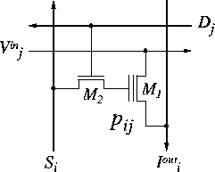
Figure 4: \
Outer-product incremental learning, using two transistors per synaptic
connection. ![]() implements a floating gate triode transconductor, and
implements a floating gate triode transconductor, and ![]() adapts the weight
adapts the weight ![]() stored on the (non-volatile) floating gate through
capacitive coupling and UV-activated oxide conduction.
stored on the (non-volatile) floating gate through
capacitive coupling and UV-activated oxide conduction.
Derivation of the gradient for recurrent networks and other systems with internal dynamics of state variables is significantly more complex, and becomes intractible for scalable VLSI implementation. Furthermore, the network model used to derive the gradient in (5) may not accurately describe the physical implementation of the network, or the characteristics of the system may not be known a priori and a model may not be available. Accurate model knowledge cannot be assumed for analog VLSI neural hardware, due to mismatches in the physical implementation which can not be predicted at the time of fabrication. This motivates the use of model-free [14] techniques that estimate gradient information from direct observation of the parameter dependence of the performance index on the physical system, rather than model-based derivation of the gradient.
Variants on the Kiefer-Wolfowitz algorithm for stochastic approximation [15], essentially implementing random-direction finite-difference gradient descent, have been formulated for blind adaptive control [17], neural networks [14],[18] and the implementation of learning functions in VLSI hardware [19],[20],[16],[21]. Algorithms under this category exhibit the desirable property that the functional form of the parameter updates is ``model-free," i.e., independent of the model specifics of the network or system under optimization. We formulate the stochastic error-descent algorithm below, as introduced in [16] for efficient supervised learning in analog VLSI.
The stochastic error-descent algorithm [16] specifies incremental updates
in the parameters ![]() as with gradient descent (5), although
using a stochastic approximation to the true gradient
as with gradient descent (5), although
using a stochastic approximation to the true gradient
where the differentially perturbed error
is obtained from two direct observations of ![]() under complementary
activation of a parallel random perturbation
under complementary
activation of a parallel random perturbation ![]() onto the parameters
onto the parameters
![]() . The perturbation components
. The perturbation components ![]() are fixed in amplitude
and random in sign,
are fixed in amplitude
and random in sign, ![]() with equal probabilities for both
polarities.
with equal probabilities for both
polarities.
The algorithm essentially performs gradient descent in random directions in the
parameter space, along the direction of the perturbation vector. As with exact
gradient descent, iteration of the updates using (6) converges in
the close proximity of a (local) minimum of ![]() , provided the perturbation
amplitude
, provided the perturbation
amplitude
![]() is sufficiently small. The rate of convergence is necessarily slower
than gradient descent, since every observation (7) only reveals
scalar information about the gradient vector in one dimension. However, the
convergence is faster than that obtained with component-wise finite difference
gradient estimates, by a factor equal to the square root of the number of
adapted parameters, owing to the parallel stochastic nature of the parameter
perturbations. A formal derivation of the convergence properties of the
stochastic error-descent algorithm can be found in [16].
is sufficiently small. The rate of convergence is necessarily slower
than gradient descent, since every observation (7) only reveals
scalar information about the gradient vector in one dimension. However, the
convergence is faster than that obtained with component-wise finite difference
gradient estimates, by a factor equal to the square root of the number of
adapted parameters, owing to the parallel stochastic nature of the parameter
perturbations. A formal derivation of the convergence properties of the
stochastic error-descent algorithm can be found in [16].
The only global operations required are the evaluations of the error function in (7), which are obtained from direct observations on the system under complementary activation of the perturbation vector. The operations needed to generate and apply the random perturbations, and to perform the parameter update increments, are strictly local and identical for each of the parameter components.
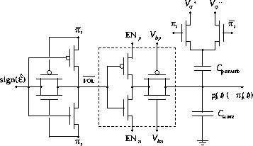
Figure 5: \
Circuit schematic of a learning cell implementing stochastic error descent,
using a hybrid binary-analog controlled charge pump adaptive element.
The circuit schematic of a learning cell implementing stochastic error descent
is given in Figure 5, adapted from [22],[23] in
simplified form. The inset of Figure 5 shows a charge pump
adaptive element, which allows independent control of the amplitude and
polarity of charge increments (4). The polarity is determined by
![]() . The amplitude of the update current
. The amplitude of the update current ![]() is
determined by gate voltages
is
determined by gate voltages ![]() and
and ![]() , biased deep in subthreshold
to allow fine (sub-fC) increments if needed. The activation of the current is
controlled by the timing of
, biased deep in subthreshold
to allow fine (sub-fC) increments if needed. The activation of the current is
controlled by the timing of ![]() and
and ![]() , switched off when
both
, switched off when
both ![]() and
and ![]() are set midway between GND and
are set midway between GND and ![]() .
Notice that the switch-off transient is (virtually) free of clock feedthrough
charge injection, because the current-supplying transistors are switched from
their source terminals, with the gate terminals being kept at constant
voltage [13].
.
Notice that the switch-off transient is (virtually) free of clock feedthrough
charge injection, because the current-supplying transistors are switched from
their source terminals, with the gate terminals being kept at constant
voltage [13].
Accordingly, the incremental update ![]() to be performed
in (7) is decomposed in amplitude and sign components. Since
to be performed
in (7) is decomposed in amplitude and sign components. Since
![]() , the amplitude
, the amplitude ![]() is global to all cells,
conventiently communicated in the form of
is global to all cells,
conventiently communicated in the form of ![]() and
and ![]() . The
(inverted) polarity
. The
(inverted) polarity ![]() is obtained as the (inverted)
exclusive-or combination of the perturbation
is obtained as the (inverted)
exclusive-or combination of the perturbation ![]() and the polarity of
and the polarity of
![]() . Since the polarity of the learning update increments is
accurately determined and implemented through binary operations, proper
convergence is guaranteed even in the presence of mismatches and offsets in the
physical implementation of the learning cell. Note that small discrepancies in
update amplitude merely affect a small change in the rate of convergence.
. Since the polarity of the learning update increments is
accurately determined and implemented through binary operations, proper
convergence is guaranteed even in the presence of mismatches and offsets in the
physical implementation of the learning cell. Note that small discrepancies in
update amplitude merely affect a small change in the rate of convergence.
The perturbation ![]() is applied to
is applied to ![]() in three phases by capacitive
coupling onto the storage node C. The binary state of the local perturbation
in three phases by capacitive
coupling onto the storage node C. The binary state of the local perturbation
![]() selects one of two global perturbation signals to couple onto C. The
perturbation signals (
selects one of two global perturbation signals to couple onto C. The
perturbation signals ( ![]() and its complement
and its complement ![]() ) globally
control the three perturbation phases
) globally
control the three perturbation phases ![]() ,
, ![]() and
and ![]() , and set the perturbation amplitude
, and set the perturbation amplitude ![]() . The simple configuration
using a one-bit multiplexer is possible because each perturbation component can
only take one of two values
. The simple configuration
using a one-bit multiplexer is possible because each perturbation component can
only take one of two values ![]() .
.
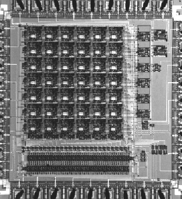
Figure: \
Micrograph of an analog VLSI recurrent neural network chip that learns
continuous-time internal dynamics using stochastic error-descent. Center:
6 ![]() 7 array of weight and threshold parameter cells with integrated
learning and storage functions. Bottom: random binary array generator
providing the parallel parameter perturbations.
7 array of weight and threshold parameter cells with integrated
learning and storage functions. Bottom: random binary array generator
providing the parallel parameter perturbations.
On-chip learning of continous-time recurrent dynamics in the state variables of an analog VLSI neural network, using stochastic error descent, has been demonstrated in [22],[23]. The chip contains an integrated network of six fully interconnected continuous-time neurons, with 42 parameters. A micrograph of the chip is shown in Figure 6. Dissipating 1.2 mW from a 5 V supply, the chip learned to regenerate at its outputs a given periodic analog target signal, representing a quadrature-phase oscillator, in 1500 training cycles of 60 msec each. The dynamic refresh scheme for long-term storage, embedded locally in the parameter cells, is described below.
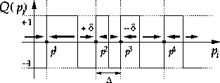
Figure 7: \
Example illustrating binary quantization Q and partial incremental refresh.
Because of the volatile nature of the adaptive element used, a dynamic refresh mechanism is required if long-term local storage of the weight values after learning is desired. A robust and efficient self-contained mechanism that does not require external storage is ``partial incremental refresh" [13]
obtained from binary quantization Q of the parameter value. Stable discrete
states of the analog dynamic memory under periodic actication of (8)
are located at the positive transitions of Q, illustrated in
Figure 7. Long-term stability and robustness to noise and errors
in the quantization requires that the separation between neighboring discrete
states ![]() be much larger than the amplitude of the parameter updates
be much larger than the amplitude of the parameter updates
![]() , which in turn needs to exceed the spontaneous drift in the parameter
value due to leakage between consecutive refresh cycles [13].
, which in turn needs to exceed the spontaneous drift in the parameter
value due to leakage between consecutive refresh cycles [13].
Partial incremental refresh can be directly implemented using the adaptive
element in Figure 5 by driving ![]() with a binary
function of the weight value [24]. As in [24], the binary
quantization function can be multiplexed over an array of storage cells, and
can be implemented by retaining the LSB from A/D/A conversion [25] of the
value to be stored. Experimental observation of quantization and refresh in
a fabricated 128-element array of memory cells has confirmed stable retention
of analog storage at 8-bit effective resolution over a time interval
exceeding
with a binary
function of the weight value [24]. As in [24], the binary
quantization function can be multiplexed over an array of storage cells, and
can be implemented by retaining the LSB from A/D/A conversion [25] of the
value to be stored. Experimental observation of quantization and refresh in
a fabricated 128-element array of memory cells has confirmed stable retention
of analog storage at 8-bit effective resolution over a time interval
exceeding ![]() refresh cycles (several days).
refresh cycles (several days).
A non-volatile equivalent of the charge-pump adaptive element used in Figure 5, which does not require dynamic refresh, is described in [9]. Correspondingly, a non-volatile learning cell performing stochastic error descent can be obtained by substitution of the core adaptive element in Figure 5. The non-volatile solution is especially attractive if long-term storage is a more pressing concern than speed of adaptation and flexibility of programming.
The examples shown demonstrate that computational primitives of adaptation, learning, and associated storage are naturally implemented in analog VLSI. The adaptation allows to compensate for inaccuracies in the physical analog VLSI implementation, besides uncertainties and fluctuations in the system under optimization.
Adaptive algorithms based on physical observation of the ``performance" gradient in the parameter space are better suited for robust analog VLSI implementation than are algorithms based on a calculated gradient. Still, care should be taken to avoid inaccuracies in the implementation of the adaptive element. Nevertheless, this can be easily achieved by ensuring the right polarity, rather than amplitude, of the parameter update increments.
The examples have been drawn from applications of supervised learning, where a teacher training signal is continuously available in the form of target outputs. The model-free approach can be extended to more general ``training-free" learning schemes, such as reward/punishment driven reinforcement learning [8].
This document was generated using the LaTeX2HTML translator Version 96.1 (Feb 5, 1996) Copyright © 1993, 1994, 1995, 1996, Nikos Drakos, Computer Based Learning Unit, University of Leeds.